Robert Triggs / Android Authority
Ever since Google switched to its custom Tensor chips in its Pixel series, some have complained about the mediocre battery life and poor thermals they provided. This was in big part because of Google’s decision to task Samsung (more specifically, its S.LSI division) with handling many of the parts of the chip’s creation process, including manufacturing. Long story short, Samsung’s recent process nodes typically underperform those of its rival TSMC.
Fortunately, Google will soon rectify that mistake by dropping Samsung and designing its upcoming chips internally. Because of that, Google will also finally switch to TSMC, which we confirmed before. One thing that remained unclear about that, however, was which exact process would be used. Today, we can answer that question, not only for the Pixel 10’s Tensor G5 but also for the Tensor G6!
Thanks to an unprecedented leak from Google’s gChips division, Android Authority has viewed credible documents that confirm the new process nodes for Google’s upcoming chips.
You're reading an Authority Insights story. Discover Authority Insights for more exclusive reports, app teardowns, leaks, and in-depth tech coverage you won’t find anywhere else.
No 2 nm, but still a great upgrade
Google Tensor G5 (codename “laguna”), likely to be the chip in next year’s Pixel 10 series, will be manufactured on TSMC’s 3 nm-class N3E — the same exact process node Apple uses for the iPhone 16 Pro’s A18 Pro and its M4 chips. This is great news because it’s probably the best process node currently available and will definitely be a massive upgrade over Samsung’s 4 nm-class 4LPE node used in the Tensor G4, both in efficiency and performance.
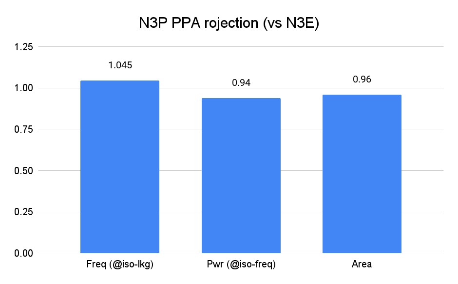
Probably the more interesting part of this leak, however, is the fact that the 2026 Tensor G6 (codename “malibu”) will be manufactured on TSMC’s upcoming N3P node, the same one rumored to be used for Apple’s A19 chip. While still a 3 nm-class node, it brings some improvements — the documents we viewed contained a chart that summarizes the changes. We are unable to share the original page. However, we recreated it below:

This might be a bit confusing, so let me give a bit of extra context: PPA stands for “Power, Performance, Area,” the three key components of any process node. The “Freq (@iso-lkg)” figure, with a 5% improvement, shows how much the frequency can be increased (which almost directly translates to performance) without affecting other characteristics of the chip (in this case, leakage, which is a concept far too complex to explain here). The second figure is “Power (@iso-freq),” which shows how much power usage can be reduced if the frequency stays the same, in this case, by 7%. It’s important to know that these two values aren’t additive — it’s either improved frequency or power usage. The last value (“Area”) shows how much smaller a finished ship can be, in this case 4%.
In summary, the Tensor G6 will also include considerable improvements to its process node, even if it is not 2nm, as previously rumored.
The use of both these process nodes shows Google is getting really serious about its upcoming Tensor chips. The previous generations were always behind in terms of the technology they used, and using a modern process node is definitely a good step in making them more competitive.
This is the first part of the series in which we will be discussing the massive Pixel leak. We will be releasing more information soon, so stay tuned!


 English (US) ·